- 您现在的位置:买卖IC网 > Sheet目录1917 > DSPIC30F4011-30I/ML (Microchip Technology)IC DSPIC MCU/DSP 48K 44QFN
dsPIC30F4011/4012
DS70135G-page 142
2010 Microchip Technology Inc.
20.4
Programming the Start of the
Conversion Trigger
The conversion trigger terminates acquisition and starts
the requested conversions.
The SSRC<2:0> bits select the source of the
conversion trigger.
The SSRC bits provide for up to five alternate sources
of conversion trigger.
When SSRC<2:0> = 000, the conversion trigger is
under software control. Clearing the SAMP bit causes
the conversion trigger.
When SSRC<2:0> = 111 (Auto-Start mode), the con-
version trigger is under A/D clock control. The SAMC
bits select the number of A/D clocks between the start
of acquisition and the start of conversion. This provides
the fastest conversion rates on multiple channels.
SAMC must always be at least one clock cycle.
Other trigger sources can come from timer modules,
motor control PWM module or external interrupts.
20.5
Aborting a Conversion
Clearing the ADON bit during a conversion aborts the
current conversion and stops the sampling sequencing.
The ADCBUFx is not updated with the partially com-
pleted A/D conversion sample. That is, the ADCBUFx
will continue to contain the value of the last completed
conversion (or the last value written to the ADCBUFx
register).
If the clearing of the ADON bit coincides with an
auto-start, the clearing has a higher priority.
After the A/D conversion is aborted, a 2 TAD wait is
required before the next sampling may be started by
setting the SAMP bit.
If sequential sampling is specified, the A/D continues at
the next sample pulse, which corresponds with the next
channel converted. If simultaneous sampling is speci-
fied, the A/D continues with the next multichannel
group conversion sequence.
20.6
Selecting the A/D Conversion
Clock
The A/D conversion requires 12 TAD. The source of the
A/D conversion clock is software selected using a 6-bit
counter. There are 64 possible options for TAD.
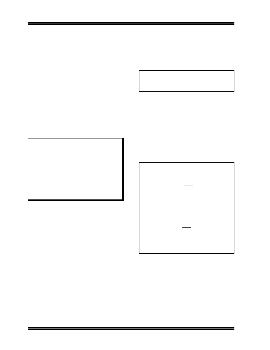
EQUATION 20-1:
A/D CONVERSION CLOCK
The internal RC oscillator is selected by setting the
ADRC bit.
For correct A/D conversions, the A/D conversion clock
(TAD) must be selected to ensure a minimum TAD time
other operating conditions.
Example 20-1 shows a sample calculation for the
ADCS<5:0> bits, assuming a device operating speed
of 30 MIPS.
EXAMPLE 20-1:
A/D CONVERSION CLOCK
CALCULATION
Note:
To operate the ADC at the maximum
specified conversion speed, the auto-
convert trigger option should be selected
(SSRC = 111) and the auto-sample
time
bits should be set to ‘1’ TAD
(SAMC = 00001). This configuration gives
a total conversion period (sample +
convert) of 13 TAD.
The use of any other conversion trigger
results
in
additional
TAD
cycles
to
synchronize the external event to the
ADC.
TAD = TCY * (0.5 * (ADCS<5:0> + 1))
ADCS<5:0> = 2
– 1
TAD
TCY
TAD = 154 nsec
ADCS<5:0> = 2
– 1
TAD
TCY
TCY = 33 nsec (30 MIPS)
= 2
– 1
154 nsec
33 nsec
= 8.33
Therefore,
Set ADCS<5:0> = 9
Actual TAD =
(ADCS<5:0> + 1)
TCY
2
=
(9 + 1)
33 nsec
2
= 165 nsec
发布紧急采购,3分钟左右您将得到回复。
相关PDF资料
DSPIC30F4013-30I/ML
IC DSPIC MCU/DSP 48K 44QFN
DSPIC30F5013-30I/PT
IC DSPIC MCU/DSP 66K 80TQFP
DSPIC30F5015-30I/PT
IC DSPIC MCU/DSP 66K 64TQFP
DSPIC30F6010-20E/PF
IC DSPIC MCU/DSP 144K 80TQFP
DSPIC30F6010A-30I/PF
IC DSPIC MCU/DSP 144K 80TQFP
DSPIC30F6013A-30I/PF
IC DSPIC MCU/DSP 132K 80TQFP
DSPIC30F6014-30I/PF
IC DSPIC MCU/DSP 144K 80TQFP
DSPIC33EP512MU814-I/PL
IC DSC 16BIT 512KB 144LQFP
相关代理商/技术参数
DSPIC30F4011-30I/P
功能描述:数字信号处理器和控制器 - DSP, DSC 16bit Signal Cntrlr RoHS:否 制造商:Microchip Technology 核心:dsPIC 数据总线宽度:16 bit 程序存储器大小:16 KB 数据 RAM 大小:2 KB 最大时钟频率:40 MHz 可编程输入/输出端数量:35 定时器数量:3 设备每秒兆指令数:50 MIPs 工作电源电压:3.3 V 最大工作温度:+ 85 C 封装 / 箱体:TQFP-44 安装风格:SMD/SMT
DSPIC30F4011-30I/PT
功能描述:数字信号处理器和控制器 - DSP, DSC 16 Bit MCU/DSP 30M 48KB FL RoHS:否 制造商:Microchip Technology 核心:dsPIC 数据总线宽度:16 bit 程序存储器大小:16 KB 数据 RAM 大小:2 KB 最大时钟频率:40 MHz 可编程输入/输出端数量:35 定时器数量:3 设备每秒兆指令数:50 MIPs 工作电源电压:3.3 V 最大工作温度:+ 85 C 封装 / 箱体:TQFP-44 安装风格:SMD/SMT
DSPIC30F4011T-20E/ML
功能描述:数字信号处理器和控制器 - DSP, DSC 16 Bit MCU/DSP 44LD 20M 48KB FL RoHS:否 制造商:Microchip Technology 核心:dsPIC 数据总线宽度:16 bit 程序存储器大小:16 KB 数据 RAM 大小:2 KB 最大时钟频率:40 MHz 可编程输入/输出端数量:35 定时器数量:3 设备每秒兆指令数:50 MIPs 工作电源电压:3.3 V 最大工作温度:+ 85 C 封装 / 箱体:TQFP-44 安装风格:SMD/SMT
DSPIC30F4011T-20E/PT
功能描述:数字信号处理器和控制器 - DSP, DSC 16 Bit MCU/DSP 20M 48KB FL RoHS:否 制造商:Microchip Technology 核心:dsPIC 数据总线宽度:16 bit 程序存储器大小:16 KB 数据 RAM 大小:2 KB 最大时钟频率:40 MHz 可编程输入/输出端数量:35 定时器数量:3 设备每秒兆指令数:50 MIPs 工作电源电压:3.3 V 最大工作温度:+ 85 C 封装 / 箱体:TQFP-44 安装风格:SMD/SMT
DSPIC30F4011T-20I/ML
功能描述:数字信号处理器和控制器 - DSP, DSC DIG SIG CONTR RoHS:否 制造商:Microchip Technology 核心:dsPIC 数据总线宽度:16 bit 程序存储器大小:16 KB 数据 RAM 大小:2 KB 最大时钟频率:40 MHz 可编程输入/输出端数量:35 定时器数量:3 设备每秒兆指令数:50 MIPs 工作电源电压:3.3 V 最大工作温度:+ 85 C 封装 / 箱体:TQFP-44 安装风格:SMD/SMT
DSPIC30F4011T-20I/PT
功能描述:数字信号处理器和控制器 - DSP, DSC 16 Bit MCU/DSP 20M 48KB FL RoHS:否 制造商:Microchip Technology 核心:dsPIC 数据总线宽度:16 bit 程序存储器大小:16 KB 数据 RAM 大小:2 KB 最大时钟频率:40 MHz 可编程输入/输出端数量:35 定时器数量:3 设备每秒兆指令数:50 MIPs 工作电源电压:3.3 V 最大工作温度:+ 85 C 封装 / 箱体:TQFP-44 安装风格:SMD/SMT
DSPIC30F4011T-30I/ML
功能描述:数字信号处理器和控制器 - DSP, DSC 16 Bit MCU/DSP 44LD 30M 48KB FL RoHS:否 制造商:Microchip Technology 核心:dsPIC 数据总线宽度:16 bit 程序存储器大小:16 KB 数据 RAM 大小:2 KB 最大时钟频率:40 MHz 可编程输入/输出端数量:35 定时器数量:3 设备每秒兆指令数:50 MIPs 工作电源电压:3.3 V 最大工作温度:+ 85 C 封装 / 箱体:TQFP-44 安装风格:SMD/SMT
DSPIC30F4011T-30I/PT
功能描述:数字信号处理器和控制器 - DSP, DSC 16 Bit MCU/DSP 30M 48KB FL RoHS:否 制造商:Microchip Technology 核心:dsPIC 数据总线宽度:16 bit 程序存储器大小:16 KB 数据 RAM 大小:2 KB 最大时钟频率:40 MHz 可编程输入/输出端数量:35 定时器数量:3 设备每秒兆指令数:50 MIPs 工作电源电压:3.3 V 最大工作温度:+ 85 C 封装 / 箱体:TQFP-44 安装风格:SMD/SMT